|
효율 높은 디스플레이를 위한 편광된 LED
렌셀러 폴리테크닉 대학교(RPI)의 스마트 조명 공학 연구 센터와 III-질화물 재료 공급자 카이마(Kyma) 기술은 0.77의 편광 세기 비율을 가지는 질화물 반도체 발광소자(LED)를 만들기 위해 비표준 결정 성장 방향들을 이용했다[Shi You et al, Appl. Phys. Express, vol3, p102103, 2010]. 연구원들은 편광 세기 비율이 평평한 표면 방출로부터 500nm 보다 긴 파장을 위해 AlGaInN LED의 상부 표면 방출에서 얻은 최고의 값이라고 전했다.
편광된 LED들은 액정 디스플레이(LCD)들에 더 효율적인 백라이트 유닛(BLU)들을 만드는데 사용될 수 있다. 네마틱 상의 액정 디스플레이들은 이미지를 만들기 위해 편광된 빛을 사용한다. 액정 물질은 두 개의 편광판 사이에 놓인다. 전계가 인가되면 액정이 움직이게 되고, 이 액정 구조의 배열 변화에 의해 빛의 편광성이 변화되어 빛의 투과도가 조절된다. 만약 편광되지 않은 빛을 사용한다면, 광원의 세기가 절반 이상 첫 번째 편광판에 의해 사라지게 될 것이다.
과거 수년간 많은 연구 그룹들은 LCD 성능을 향상시키기 위해 통상의 c-방향과 다른 결정 방향들로 성장된 질화물 반도체 LED들을 연구해 왔다. 특히, c-방향으로 배열하게 하는 전기적 편광계들로부터 증가하는 구동 전류로 출력광 내의 파장 이동을 피하기 위해 c-방향과 다른 결정 방향들로 성장된 질화물 반도체 LED들을 연구해 왔다. 이때 무극성과 반극성 방향에서 성장된 LED들은 선형적으로 편광된 빛으로 발생한다.
렌셀러와 카이마 연구원들은 수소 기상 증착법(HVPE)을 이용하여 c-방향에서 성장된 독립된 벌크 웨이퍼들(50mm 반경, 7mm 두께 이상)에서 잘린 5mm×10mm 직각 슬라이스들인 갈륨 질화물(GaN) 기판들을 사용했다. 이 연구는 0.2도 이하의 오프 컷(off-cut)을 가진 표면이 m-과 a-면들인 기판들을 이용했다. 화학적-기계적 연마는 양면 위에 0.5nm 제곱 평균(rms) 이하인 표면 거칠기를 가지게 하였다.
LED 구조들은 금속 유기 화학 증착법(MOCVD)을 통해 성장하였다. 다중 양자 우물(MQW) 발광 활성 영역들은 5내지 8층의 인듐 갈륨 질화물(InGaN) 우물들과 GaN 장벽들로 이루어졌다.
인듐 함량과 우물/장벽 두께는 엑스레이 회절(XRD)과 고분해 투과 전자 현미경 (HR-TEM)에서 얻은 정보를 조합하여 결정되었다. 우물 두께는 3~4nm 영역이고 장벽은 20~25nm였다. MQW 층들의 잔류 거칠기는 원자력 현미경(AFM)으로 측정되었다. 이때, a-시편들에서는 1.2~3.0nm rms, m-시편들에서는 0.2~0.5nm rms였다.
n-형 주입 영역은 기판 위에 먼저 성장되었고 실리콘이 도핑된 GaN의 1μm로 구성되었다. 그 위에 MQW가 위치하였다.
광발광(PL) 연구들은 a-면 시편들에 비해 30% 더 높은 편광률을 m-면 MQW 구조가 가진다는 것을 보였다. 연구원들은 현재 이론은 이 결과를 예측하지 못하고 있고 a-구조들의 더 높은 거칠기 값들은 비등방성 변형 효과와 밸런스 밴드 구조의 이동과 분할을 통해 출력광의 편광성이 주로 영향을 준다고 생각되는 구속 효과의 완화 때문이라고 제안하고 있다.
m-면 MQW 구조들 중 하나의 전계발광(EL)은 온전한 LED를 만들기 위해 15nm AlGaN 전자차단층과 120nm p-GaN 주입층이 추가되어 연구되었다. a-와 c-축을 따른 이 편광 성분들은 파장 영역 전체에서 20mA 주입 전류에서 측정되었다.(그림1)

그림1: (a) 20mA에서 m-면 LED의 편광 분해
EL 스펙트럼들. 방출은 491nm에서 최고 세기를
가지는 c-축 피크들을 따라 편광되었다.
반면 a-축을 따라 편광된 방출은 505nm에서 피크를 가진다.
(b) 두 주된 수직 요소들 모두의 보간법으로
편광각 모두의 함수에 따른 EL 세기.
0도와 180도에서 편광판은 c-축을 따른다.
그리고 90도에서는 a-축을 따른다.
a-방향에 수평된 전계를 가진 광편광은 505nm(청녹색)에서 피크를 가졌다. 반면 c-편광은 훨씬 더 작고(a-피크의 약 13%) 더 짧은 피장인 491nm에 중심을 두었다. 이 더 짧은 파장은 이 방향에서 약 70meV의 에너지 전환 증가를 가르킨다. 변형 효과에 의한 분할에 기초를 둔 이론적인 예측은 40meV였다. 이 차이는 양자구속효과에 의한 것으로 추측된다.
이 팀은 더 큰 편광은 적당한 패키징과 다이 끝 방출 억제로 이뤄질 수 있을 것이라고 한다. 편광성의 각 의존성은 또한 a-와 c-방향들에 평형인 분리된 성분들에 의한 두 세기의 가정에 맞는다. LED 내에 내부 산란된 빛으로부터 불규칙 기여는 매우 작게 된다. 연구원들은 더 긴 파장으로 움직임이 (예를 들어 약 530nm에서 녹색 또는 550nm에서 진한 녹색) 특별히 m-면 구조들을 위한 편광률을 증가시킬 수 있다고 기대한다.
표준 c-면과 m-면 LED들에서의 방출에 대한 선형 편광판들의 효과 또한 비교되었다. (그림2) c-면 방출은 57.7%로 줄었다. 반면 m-면 LED의 손실은 단지 25.4%였다. m-면 LED들에서의 편광된 빛의 사용은 출력 소비를 점재적으로 줄이는 편광된 시스템들의 출력 효율을 증가시킬 수 있다. 마지막 실험에서 발생한 0.77 편광된 빛의 경우 같은 편광된 출력이 표준 c-면 LED에 비교하여 44% 작은 입력 광으로 성취될 수 있을 것이다.

그림2: 평관판을 가지거나 가지지 않은
(a) c-와 (b) m- 면 LED들
원문>>
22 October 2010
Polarized LED from Rensselaer and Kyma raises hope of more efficient displays
The Smart Lighting Engineering Research Center (ERC) at Rensselaer Polytechnic Institute (RPI) in Troy, NY and III-nitride materials provider Kyma Technologies Inc of Raleigh, NC, USA have used non-standard crystal growth directions to create a nitride semiconductor light-emitting diode with a polarization intensity ratio of 0.77 [Shi You et al, Appl. Phys. Express, vol3, p102103, 2010]. The researchers comment that this polarization intensity ratio is, to their knowledge, “the highest value obtained in top surface emission of any AlGaInN LED for wavelengths longer than 500nm from planar surface emission”.
Polarized LEDs could be used to make more efficient back-lighting units for liquid-crystal displays (LCDs). Nematic-phase liquid-crystal displays use polarized light to create images. The liquid-crystal material is put between a pair of polarizers. By varying the configuration of the liquid-crystal structure under an applied electric field, the light’s polarization can be shifted, thus modulating the transmission. If this set-up is driven by unpolarized light, then more than half the source’s power is thrown away by the first polarizer.
In the past couple of years, a number of research groups have been investigating nitride semiconductor LEDs grown in crystal directions different from the usual c-direction to improve performance, in particular to avoid wavelength shifts in the output light with drive current arising from the electric polarization fields that are directed in the c-direction in these structures. LEDs grown in non-polar and semi-polar directions also produce linearly polarized light.
The Rensselaer and Kyma researchers used gallium nitride (GaN) substrates that were 5mm x 10mm rectangular slices cut from free-standing bulk wafers (50mm diameter, up to 7mm thick) grown in the c-direction using hydride vapor phase epitaxy (HVPE). The study used substrates with surface m- and a-planes with off-cut angle less than 0.2°. Chemo-mechanical polishing was used to reduce the surface roughness to less than 0.5nm root-mean-square (rms) on both sides.
The LED structures were grown using metal-organic chemical vapor deposition (MOCVD). The multi-quantum well (MQW) light-emitting active regions consisted of five or eight pairs of indium gallium nitride (InGaN) wells and GaN barriers.
The indium fraction and well/barrier thicknesses were determined by combining information from x-ray diffraction (XRD) and high-resolution transmission electron microscopy (HR-TEM). The well thicknesses were in the range 3–4nm and the barriers were 20–25nm. The residual roughness of the MQW layers was determined by atomic force microscopy (AFM) – in the a-samples the value was 1.2-3.0nm rms and in the m-samples it was 0.2-0.5nm rms.
The n-type injection region was grown first on the substrate and consisted of 1μm of silicon-doped GaN. This was followed by the MQW sequence.
Photoluminescence (PL) studies show the m-plane MQW structures to have a polarization ratio that is about 30% higher than that for the a-plane samples. The researchers comment that current theory does not predict this, and suggest that the higher roughness values of the a-structures could be due to relaxation of the anisotropic strain effects and confinement that are thought to affect mainly the polarization of the output light through shifts and splitting of the valence band structure.
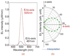
Figure 1: (a) Polarization-resolved EL spectra of m-plane LED at 20mA. Emission polarized along the c-axis peaks with maximum intensity at 491nm, while emission polarized along the a-axis has a peak at 505nm. (b) EL intensity as a function of polarization angle together with interpolation of both main perpendicular components. At 0° and 180°, the polarizer is along the c-axis, and at 90° it is along the a-axis.
The electroluminescence (EL) of one of the m-plane MQW structures was studied by adding a 15nm AlGaN electron-blocking layer and 120nm p-GaN injection layer to complete it into an LED. The polarization components along a- and c-axes were measured at an injection current of 20mA over a range of wavelengths (Figure 1).
The light polarization with the electric field parallel to the a-direction had a peak at 505nm (blue-green), while the c-polarization was much smaller (about 13% of the a-peak) and centered at a shorter wavelength 491nm. This shorter wavelength indicates an energy transition increase of ~70meV in this direction. Theoretical predictions based on splitting due to strain effects would give 40meV. The discrepancy could be due to quantum confinement effects.
The team expects that higher polarization could be achieved with proper packaging and suppression of die edge emission. The angular dependence of the polarization also fits the assumption of two intensities coming from separate components parallel to the a- and c-directions. The random contribution from light internally scattered within the LED is described as being ‘very low’. The researchers hope that moving to longer wavelengths (e.g. green at ~530nm or deep green at ~550nm) could increase the polarization ratio, particularly for m-plane structures.
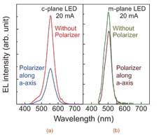
Figure 2: EL spectra of (a) c- and (b) m-plane LEDs with and without polarizer.
The effect of linear polarizers on the emissions from standard c-plane and m-plane LEDs were also compared (Figure 2). The c-plane emission was reduced by 57.7%, while the loss for the m-plane LED was only 25.4%. The use of polarized light from m-plane LEDs could enhance the output efficiency of polarized systems, potentially reducing power consumption. In the case of the 0.77 polarized light created in their latest experiments, the researchers say that the same polarized output power could be achieved with 44% less input light power, compared with a standard c-plane LED.
| 