|
타이완의 연구원들은 20mA 구동 전류에서 일반적인 사파이어에 성장된 소자에 비해 2.4배 외부양자효율 (EQE) 향상된 질화물 반도체 LED의 사파이어 나노패터닝 기술을 개발했다. [Yu-Sheng Lin and J. Andrew Yeh, Appl. Phys. Express, vol4, p092103, 2011] 국립 칭화 대학과 국립 응용 연구소의 연구원들은 EQE 40-50% 영역에서 나노 패턴된 사파이어 가판들 상에 보고된 다른 소자들에 비해 20mA에서 58.3%의 EQE를 가진다고 밝혔다. 일반적인 소자는 24.5% EQE를 가진다. 소자 상부에서 측정된 광출력은 20mA에서 패턴된 소자의 경우, 33.1mW로 일반적인 LED의 13.9mW에 비해 크게 향상되었다.
많은 연구원들은 질화물 반도체 LED의 성능을 향상시키는 저렴한 방법을 찾고 있다. 이를 위한 한가지 기술은 질화물 성장 전에 사용되는 사파이어 기판을 패턴을 주는 것이다. 이 나노 크기 패턴들은 결과적으로 LED의 성능 향상을 위해 두 가지 효과들을 준다. 첫 번째로, 나노 패턴된 표면은 질화물 반도체 결정 내 전위들의 수를 감소시키는 성장 과정에 영향을 준다. 여기서 전위들은 LED 성능을 감소시킬 수 있다. 두 번째로, 성장 과정이 사파이어와 질화물 반도체 헤테로구조 사이 계면에서 공기-구멍들을 흔히 만들어 낸다. 이 구멍들은 LED 작동에 의해 발생된 빛이 소자를 벗어나게 경로를 개선하는데 사용될 수 있다. 때때로, 두 효과들 모두가 질화물 LED의 EQE를 개선하기 위해 작용한다.
타이완 연구원들은 구멍이 포함된 외피 같은 나노구조 (VECN)라 불리는 무질서한 나노패터닝을 이용했다. 이 연구팀은 고가 반도체 마스크의 사용 없이 고효율 LED를 위해 사파이어 상에 기판 수준 외피 같은 나노구조가 가격 효율적인 해법이라고 믿는다.
사파이어 기판 표면의 나노패터닝은 2μm 두께의 다결정 실리콘 하드마스크를 만들고 보론 테트라클로라이드와 클로린 혼합을 이용하여 유도 결합 플라즈마 반응성 이온 식각을 실행하여 개발되었다. 다결정 실리콘은 640°C 저기압 화학 증착법으로 증착 되었다. 이 하드마스크에 대한 패터닝은 30분 동안 희석된 라이트(Wright)-식각 용액 에서 다결정 실리콘이 덮힌 기판을 담금으로써 형성시켰다. 라이트-식각 용액은 실리콘 결정 구조 내 결점들을 밝히기 위해 1970대 개발된 산성 혼합물이다. 이 하드마스크는 80°C에서 칼륨 수산화 용액으로 제거되었다. 이 사파이어 기판 표면 패터닝은 50-150nm 떨어져 있고 80-150nm 짚은 구조를 가진 10^10/cm^2 로 구성된다.
그림1 : (a) 구멍이 포함된 외피 나노구조 (VECN)을 가진 사파이어, (b) VECN 사파이어 상의 도핑되지 않은 갈륨 질화물 (u-GaN), (c) 일반적인 사파이어 상의 u-GaN 표면들의 AFM 이미지들. 스캔 면적은 5μm x 5μm이다.
이 LED 구조들은 저기압 금속-유기 화학 증착법을 이용하여 성장되었다.
그림 2 : LED-VECN 구조의 개략도. p-측의 층등은 30nm 알루미늄 갈륨 질화물/갈륨 질화물 (AlGaN/GaN) 초격자(superlattice)와 100nm p-GaN으로 구성된다. 버퍼(buffer) 층의 원자 힘 현미경 (AFM)는 10^7?10^8/cm^2의 구멍 밀도를 나타낸다. 이 결과는 일반적인 사파이어 기판 (CSS) 상에 성장된 갈륨 질화물 (GaN)의 구멍 밀도치 보다 100 배 적은 것이다. 이 구멍들은 사파이어에서 GaN 표면의 상부로 전해지는 쓰레딩 (threading) 전위들에 의한 것이다.
GaN/CSS의 경우, 294 아크세크 (arcsec)과 비교하여 나노패턴된 GaN/사파이어의 경우, 211 아크세크의 x-선 회절 (0002) 락킹(rocking) 곡선 반치폭은 결정질이 개선되었다는 것을 보여준다. 상부 LED 층들은 216 아크세크까지 나노패턴된 소자 구조의 경우, FWHM이 약간 증가했지만, CSS 소자 구조 FWHM은 256 아크세크까지 감소했다. 위성 피크들은 5차까지 보였다. 이것은 소자의 활성영역을 이루는 인듐 갈륨 질화물/갈륨 질화물 (InGaN/GaN) 다중 양자 우물들 (MQW)에 대해 훌륭한 층 주기성을 보여준다.
전계 발광 피크는 20mA 구동 전류에서 438nm (보라색)에서 나타났다.
그림 3 : (a) 20mA의 주입 전류 하에서 438nm에 위치한 VECN과 일반적인 (CSS) 기판 상 LED 전계발광 스펙트럼들. (b) LED-VECN과 LED-CSS의 전류-전압 (I-V) 곡선들, LED-VECN과 LED-CSS의 전류 특성에 따른 (c) 광출력과 (d) EQE. (그림3) 20mA에서 패턴된 LED는 일반적은 소자의 3.8 V에 비해 3.6 V의 더 낮은 순방향 전압을 가졌다. GaN/사파이어 계면의 반사는 일반적인 사파이어에 비해 패턴된 소자에서 32.8% 더 높았다. 이 반사는 GaN 성장 중 형성된 공기 구멍에서 발생한다고 믿어진다. 이런 반사는 GaN (2.45)와 공기 (~1) 사이 굴절률의 큰 차이로 인해 발생한다.
결정구조와 광 반상의 특성들은 전위 밀도 감소와 반사를 통해 향상된 광추출을 나타냈다.
|


<원문>EQE increased 2.4-fold with void-embedded cortex nano-patterned LED
Taiwan-based researchers have developed a sapphire nanopatterning technique that increases external quantum efficiencies (EQE) of nitride semiconductor LEDs by 2.4x over devices grown on conventional sapphire at 20mA drive current [Yu-Sheng Lin and J. Andrew Yeh, Appl. Phys. Express, vol4, p092103, 2011].
The researchers at National Tsing Hua University and National Applied Research Laboratories comment that the EQE of 58.3% at 20mA is comparable with that of other reported devices on nanopatterned sapphire substrates with values in the range 40–50%. The conventional device had an EQE of 24.5%. The output power measured from the top side of the devices at 20mA was 33.1mW for the patterned device and 13.9mW for the conventional LED.
Many researchers are seeking low-cost ways to enhance the performance of nitride semiconductor LEDs. one technique for this has been to pattern the sapphire substrate used before nitride growth. These nano-scale patterns can have two effects to improve the performance of the resulting LEDs.
First, the nanopatterned surface affects the growth process, reducing the number of dislocations in the nitride semiconductor crystal; such dislocations can degrade LED performance. Second, the growth process often creates air-voids at the interface between the sapphire and nitride semiconductor heterostructure; the voids can be used to alter the way the light generated by the LED action leaves the device. Sometimes both effects operate to improve EQEs of nitride LEDs.
The Taiwan researchers used a random nanopatterning that they called ‘void-embedded cortex-like nanostructures’ (VECN). The team sees their method as being “a cost-effective solution to the wafer-level cortex-like nanostructures on sapphire for high-efficiency LEDs without implementation of an expensive semiconductor mask”.
The nanopatterning of the sapphire wafer surface was achieved by creating a 2μm-thick hard mask of polysilicon and performing an inductively coupled plasma reactive-ion etch with a boron tetrachloride and chlorine mix. The deposition of the polysilicon was through 640°C low-pressure chemical vapor deposition. The patterning for the hard mask was created by dipping the polysilicon-covered wafer in diluted Wright-etch solution for 30 minutes. Wright-etch solution is an acid mix developed in the 1970s to reveal defects in silicon crystal structures. The hard mask was removed by potassium hydroxide solution at 80°C. The resulting patterning of the sapphire wafer surface consisted of 1010/cm2 80–150nm deep structures spaced 50–150nm apart (Figure 1).
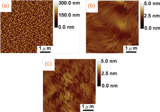
Figure 1: AFM images of surfaces of (a) sapphire with void-embedded cortex-like nanostructure (VECN), (b) undoped gallium nitride (u-GaN) on VECN sapphire, and (c) u-GaN on conventional sapphire. Scan area is 5μm x 5μm.
The LED structures were grown using low-pressure metal-organic chemical vapor deposition (Figure 2). Atomic force microscopy (AFM) of the buffer layer suggested a pit density of 107–108/cm2. This is two orders of magnitude lower than pit density values for gallium nitride (GaN) grown on conventional sapphire substrates (CSS). Such pits are attributed to threading dislocations that propagate from the sapphire to the top of the GaN surface.
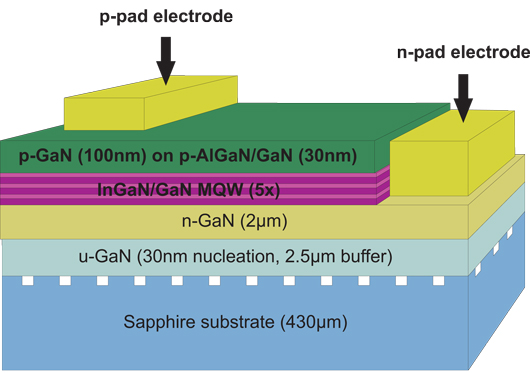
Figure 2: Schematic diagram of LED-VECN structure. The p-side layers consist of 30nm aluminum gallium nitride/gallium nitride (AlGaN/GaN) superlattice and 100nm p-GaN.
X-ray diffraction (0002) rocking curve full-width at half maximum (FWHM) values of 211 arcsec for the nanopatterned GaN/sapphire, compared with 294 arcsec for GaN/CSS, also suggest improved crystal quality. The further LED layers slightly increased the FWHM for the nanopatterned device structure to 216 arcsec, while the CSS device structure FWHM decreased to 256 arcsec. Satellite peaks up to fifth order were detected, suggesting good layer periodicity for the indium gallium nitride/gallium nitride (InGaN/GaN) multi-quantum wells (MQW), which made up the active region of the device.
The electroluminescent peak occurred at 438nm (violet) at 20mA drive current (Figure 3). At 20mA, the patterned LED had a lower forward voltage of 3.6V, compared with the conventional device’s 3.8V. The reflection from the GaN/sapphire interface was 32.8% higher in the patterned device compared with that on conventional sapphire. The reflection is thought to occur at air voids formed during the GaN growth. Such reflection occurs due to the large difference in refractive index between GaN (2.45) and air (~1).
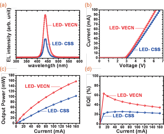
Figure 3: (a) Electroluminescence spectra for LED on VECN and conventional (CSS) substrate located at 438nm under an injection current of 20mA. (b) Current–voltage (I–V) curves of the LED-VECN and the LED-CSS, (c) light output power, and (d) EQE in relation to current characteristics of LED-VECN and LED-CSS, respectively.
The characterizations of the crystal structure and light reflection suggest that the improvement results from both reduction in dislocation density, and improved light extraction through reflection.
Nano-patterned LEDs AlGaN/GaN Sapphire substrates
'LED 새소식 > LED NEWS' 카테고리의 다른 글
| LED 조명의 리스크 (0) | 2011.09.16 |
|---|---|
| 양자점 LED (0) | 2011.09.16 |
| 다가올 시장 대비한 기술 개발에 매진해야 (0) | 2011.09.16 |
| 스필LED, 친환경·완전방수 LED컨버터 ‘스필파워’ 출시 (0) | 2011.09.15 |
| LG전자, 평택市에 ‘미래성장동력 산업단지’ 조성 (0) | 2011.09.15 |